Experimenting with Feedback and Crossover Distortion
I was experimenting with some analog circuits and, while reading this article, built a test circuit to better understand how an operational amplifier maintains linearity using negative feedback. During this process, I ended up generating enough material for a short article—so I wrote one, hoping it might be interesting to someone. I also made a video, a link to which is available at the end of the article.
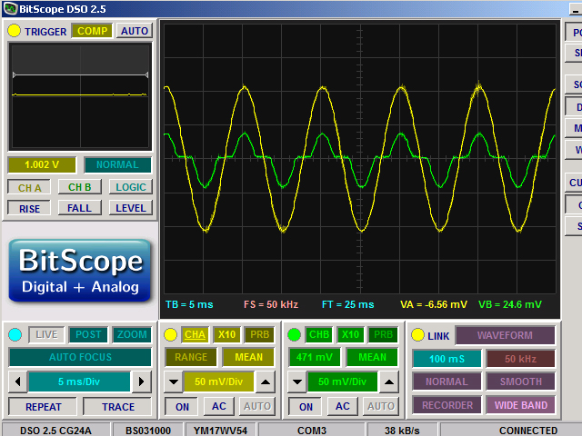
When driven by a sine wave, a push-pull stage constructed from a PNP/NPN transistor pair exhibits what's known as “crossover distortion” (see the linked Wikipedia article). This occurs due to a dead band—a region on the waveform between negative VBE and positive VBE where both transistors are off and do not conduct, effectively doing nothing. The green oscilloscope trace in the title image shows the resulting distorted waveform. I breadboarded a modified version of the circuit from the Wikipedia article to generate the waveforms. I also created an LTspice model—it can be useful if you don’t have the components to build the circuit or want to study aspects of the circuit that are difficult to measure in real life. LTspice is available for free from Analog Devices (formerly Linear Technology).
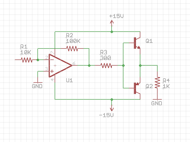
 A few notes about the circuit: For the frequencies I’m using, none of the component values are critical. I used a TL081 op-amp and 2N3904/2N3906 transistors, but other similar parts will work as well. For the LTspice model, I simply used a randomly selected op-amp from Linear’s library, and the simulation results closely matched those of the real circuit. I’ll be using the simulation for the remainder of the article, but the real circuit can be seen in the video.
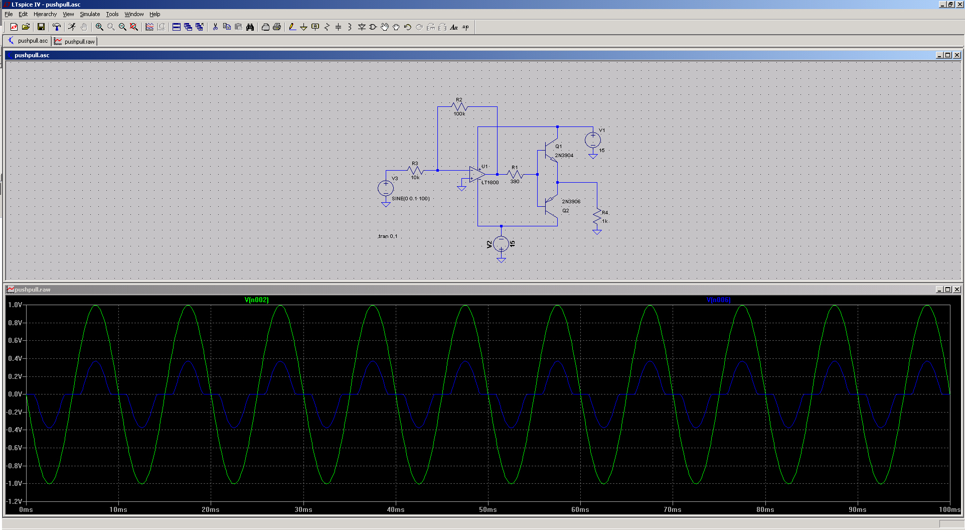
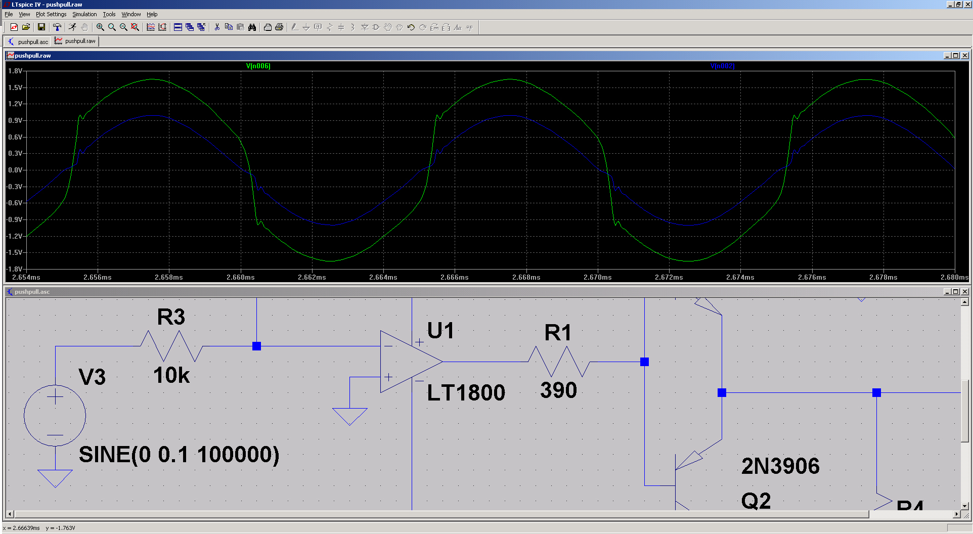
When we load the model into LTspice, run the simulation, and probe the op-amp output and the push-pull output, we get waveforms like the ones in the screenshot on the left. The green waveform is the op-amp output; the blue one is from the power stage. As long as it's operating within specified limits, the op-amp remains quite linear, so it faithfully reproduces the input sine wave. However, the power stage, driven by the op-amp, cannot reproduce the signal accurately when the input falls within the dead band.
 We know that the concept of negative feedback originally came to Harold Black when he was trying to solve a very similar problem—how to keep a circuit linear while using non-linear components. In our real circuit, the transistors aren’t matched, and we can observe that, in addition to the crossover distortion, the negative half of the waveform has a larger amplitude. In contrast, the simulated waveform is perfectly symmetrical—just one reason why simulation results should always be treated with caution.
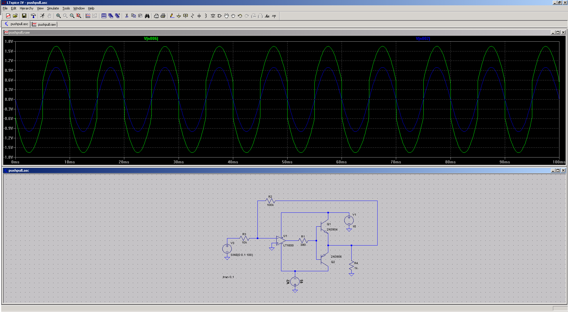
Let’s now modify the circuit by moving the right end of the feedback resistor to the output of the power stage. This allows the op-amp to sample the actual output and attempt to correct it. The result is shown in the screenshot on the right. The op-amp output now sprints through the dead band as quickly as its slew rate allows, resulting in an output waveform that is much closer to a true sine wave.
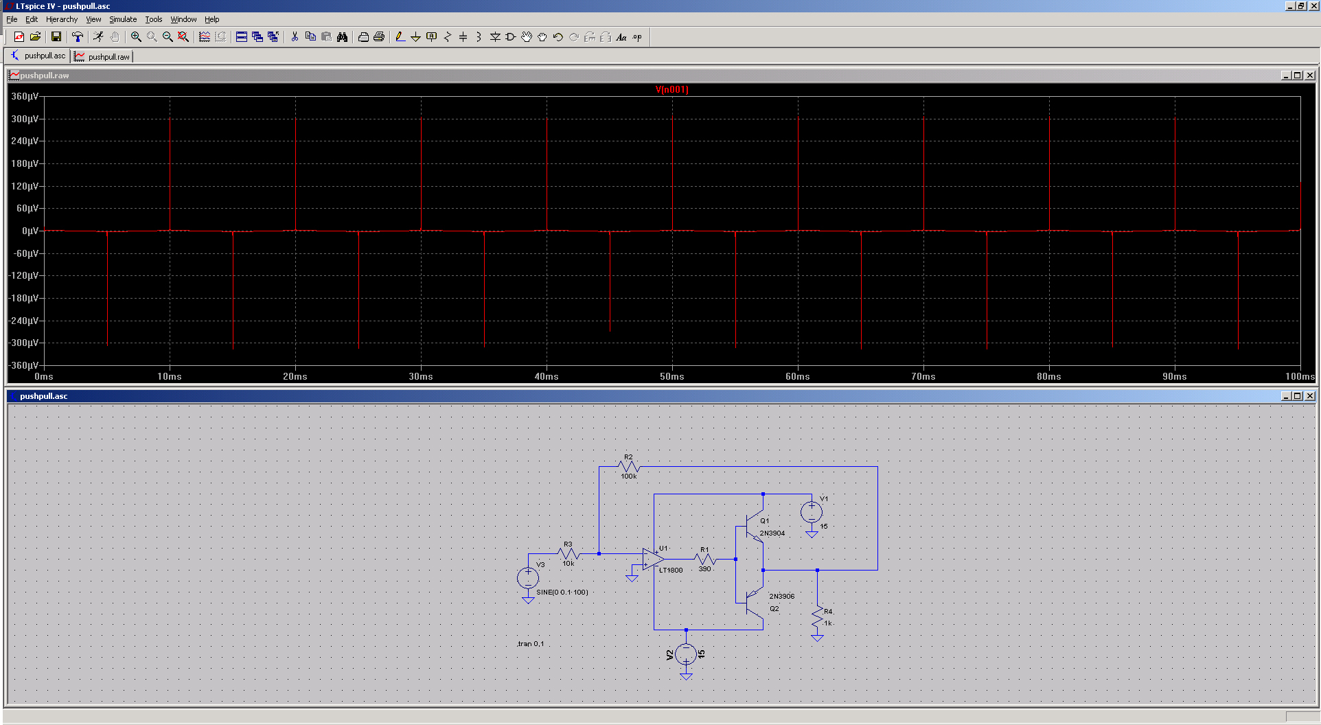 To understand this behavior better, let’s take another measurement (and another screenshot, visible on the left). Here, the red trace shows the voltage at the op-amp’s inverting input. This is the sum of the generator signal and the output signal, which is out of phase with the input—so the red waveform effectively represents the difference between them. Most of the time, this difference is very small, appearing as a nearly straight line. However, at the start of the dead band, the difference between input and output increases, and the resulting vertical spike drives the op-amp output, correcting the transistor non-linearity.
Notice the peak-to-peak amplitude of this signal. Measuring a 300 µV difference like this on real hardware is difficult, as it's well below the sensitivity of most oscilloscopes. This is where simulators excel—any signal, no matter how small or fast, can be easily visualized. If you're curious, try probing other points in the circuit, like voltages across resistors or currents at the transistor terminals.
 Finally, by modifying the model once more, we can observe a limitation of the op-amp. When I increased the input frequency to 100 kHz, the op-amp began struggling to keep up due to its finite slew rate—and the distortion returned.
That’s all! Play with the model, watch the video, and have fun!